
A deep dive into System Basis Chips for Battery Management Systems where efficiency is not just a spec, it is survival.
The Unsung Hero of Your Battery Pack
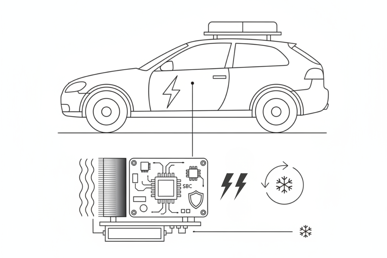
Ask any EV engineer about their Battery Management System (BMS), and they will talk about state-of-charge algorithms, cell balancing strategies, and thermal modeling. But there is a component sitting at the heart of every BMS that rarely gets the attention it deserves: the System Basis Chip (SBC).
Think of the SBC as the BMS's life-support system. While your microcontroller is busy calculating cell voltages and managing contactors, the SBC is doing the unglamorous but critical work: providing rock-solid power, watching for failures, and ensuring the system fails safely when things go wrong.
In a BMS arguably the most safety-critical ECU in an electric vehicle choosing the wrong SBC is not just a poor design decision. It is a ticking time bomb of thermal issues, parasitic battery drain, and potential safety certification nightmares.
Today, we are dissecting three leading ASIL D-capable SBCs for high-voltage BMS applications: NXP's FS26, Infineon's TLF35584QVVS2, and Texas Instruments' TPS653852A-Q1. More importantly, let's see why architectural choices at the silicon level have profound consequences for your BMS in the real world.
Why Your BMS Is Different (And Why It Matters)
Before we dive into the chips, let's acknowledge what makes a BMS unique:
It never truly sleeps. Your BMS is always on, monitoring cells, watching temperatures, waiting for a wake-up signal. Every milliwatt of parasitic drain chips away at your 12 V auxiliary battery.
It lives in thermal hell. Sealed enclosures, proximity to high-voltage battery packs, under-hood or under-seat mounting your BMS does not have the luxury of active cooling in most designs.
It must be bulletproof for years. Battery packs outlive most other vehicle components. Your SBC needs to maintain ASIL D integrity across thousands of charge cycles, temperature extremes, and electrical transients.
The Architecture That Changes Everything
Three Philosophies, Three Trade-offs
The fundamental difference between these three chips is how they convert your 12 V auxiliary battery voltage into the clean, stable power rails your BMS microcontroller needs.
NXP FS26: The Direct Buck Approach
The FS26 uses synchronous buck converters (3.7 to 6.35 V, up to 1.5 A) to directly generate the main power rails with minimal conversion stages. The strategic advantage: it includes an external boost controller (VBST) that activates only during cold-crank events, providing resilience when your 12 V auxiliary battery sags without adding continuous conversion losses.
During a cold-crank event when your 12 V auxiliary battery can drop to around 3.2 V the FS26's boost controller kicks in to maintain critical monitoring functions. This gives you the efficiency of direct buck conversion during normal operation, with cold-crank protection only when needed.
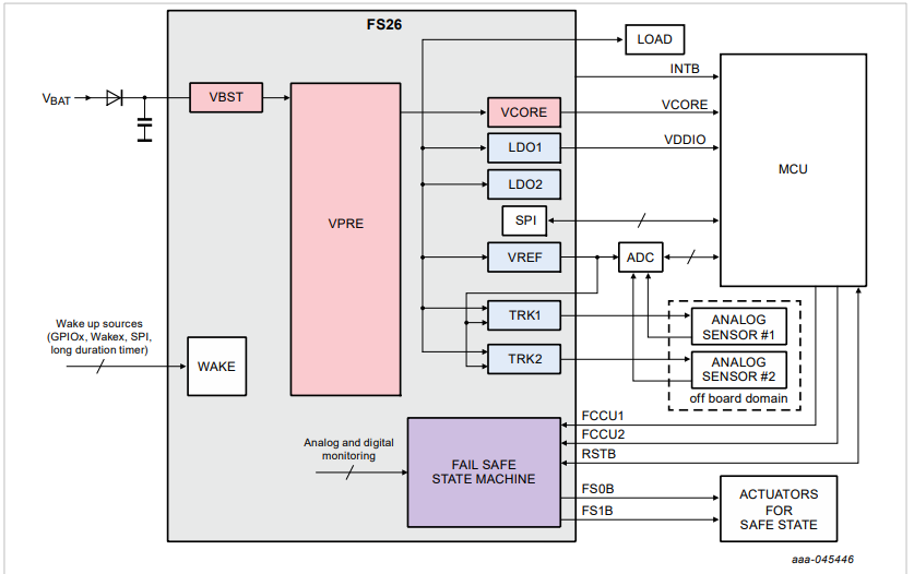
Image Source and more info - FS26
Infineon TLF35584: The Precision Multi-Rail Specialist
Infineon's approach: a serial step-down/step-up pre-regulator creates a stable intermediate voltage, which then feeds multiple ultra-precise LDO regulators. This architecture excels when you need numerous independent, low-noise rails for complex, high-performance MCUs with demanding ripple and PSRR requirements.
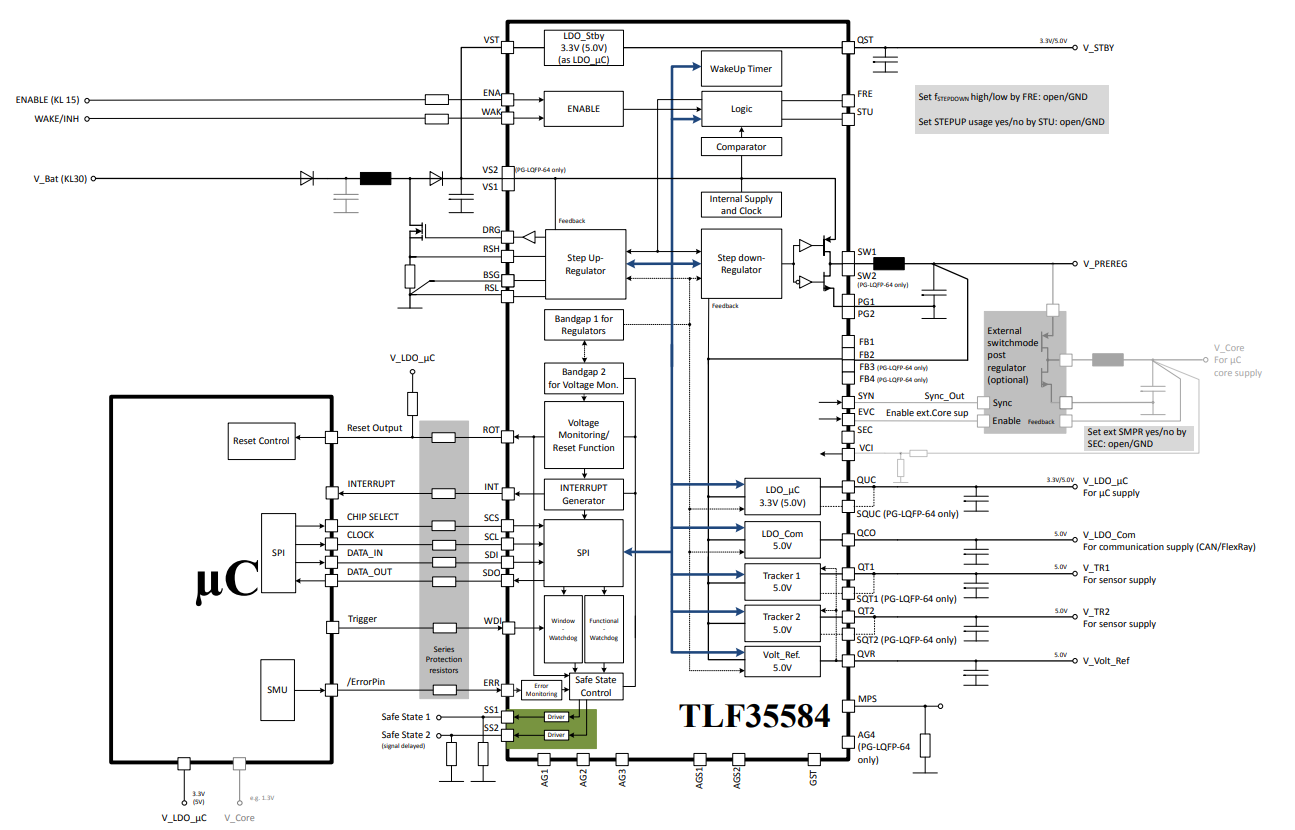
Image Source and more info - TLF35584QVVS1XUMA2
It is powerful, precise, and perfect for computational heavy-hitters but that precision comes at a thermal cost. The pre-regulator requires at least 6 V to operate, meaning deep cold-crank scenarios require external battery protection or alternative power architectures.
Texas Instruments TPS653852A-Q1: The Integrated Powerhouse
TI uses a buck-boost pre-regulator to generate a stable intermediate rail (typically 6 V), which then supplies several LDOs for final regulation. This topology offers excellent protection against voltage transients and the widest operating range of the three capable of sustaining operation down to approximately 2.3 V after initial wake-up, though requiring about 7 V for cold startup.
Here is the strategic differentiator: the TPS653852A-Q1 is the only device in this comparison with integrated CAN transceivers (3× high-speed, 3× low-speed channels), eliminating external transceiver costs and board space. However, like the Infineon, it relies on LDOs for high-current final stages, which impacts overall thermal efficiency.
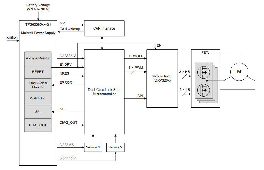
Image Source and more info - TPS653850A-Q1
The Math That Will Change How You Think About Power
Let's run the numbers for a typical BMS operating scenario. These calculations assume standard operating conditions actual results will vary with load current, input voltage, switching frequency, and PCB layout.
The Test Case: A Realistic BMS Load
Given:
1. Input Voltage: 13.5 V (typical 12 V rail)
2. Required Outputs:
Rail 1: 5.0 V @ 200 mA → 1.0 W (MCU I/O and peripherals)
Rail 2: 3.3 V @ 400 mA → 1.32 W (MCU core)
3. Total Useful Output Power: 2.32 W
Scenario 1: Pre-Regulator + LDO Architecture (TI & Infineon)
The buck-boost pre-regulator first converts 13.5 V down to approximately 6 V, then the LDOs drop from 6 V to the final voltages.
LDO Input Power (from 6 V rail):
1. 5.0 V rail: 6 V × 0.2 A = 1.2 W (only 1.0 W delivered; 0.2 W lost as heat)
2. 3.3 V rail: 6 V × 0.4 A = 2.4 W (only 1.32 W delivered; 1.08 W lost as heat)
3. Total drawn from 6 V rail: 3.6 W
Battery Input Power (assuming 85% pre-regulator efficiency): 3.6 W / 0.85 = 4.24 W
Total Power Loss (Heat): 4.24 W - 2.32 W = 1.92 W dissipated
This represents approximately 45% system efficiency. Nearly 2 watts of heat must be managed in your sealed BMS enclosure.
Scenario 2: Direct Buck Architecture (NXP FS26)
With synchronous buck converters operating at approximately 90% efficiency, each rail is converted directly from the 12 V input.
Power from Battery:
1. 5.0 V rail: 1.0 W / 0.90 = 1.11 W
2. 3.3 V rail: 1.32 W / 0.90 = 1.47 W
3. Total: 2.58 W
Total Power Loss (Heat): 2.58 W - 2.32 W = 0.26 W dissipated
Let That Sink In: approximately 1.9 W vs 0.26 W
The FS26 generates roughly 7× less waste heat in this configuration a dramatic advantage that compounds over the life of your BMS.
Architecture | Input Power | Output Power | Power Loss | System Efficiency |
Pre-reg + LDO (TI/Infineon) | 4.24 W | 2.32 W | 1.92 W | approximately 55% |
Direct Buck (NXP FS26) | 2.58 W | 2.32 W | 0.26 W | approximately 90% |
Note: These figures assume standard operating conditions. Actual efficiency varies with input voltage, load current, PCB layout, and component selection. However, the fundamental architectural advantage of direct buck conversion versus buck-boost + LDO remains consistent across operating conditions.
This architectural advantage cascades through your entire BMS design:
Thermal Benefits:
1. Junction temperatures reduced by 30 to 50°C in typical installations
2. Simplified thermal management (often eliminating heatsinks entirely)
3. Improved component reliability and longer MTBF
System Benefits:
1. Lower parasitic drain on the 12 V auxiliary battery
2. Extended sleep-mode battery life
3. Reduced cooling requirements and lower overall system cost
Real-World Impact: In a BMS that operates 24/7, that efficiency difference translates to approximately 1.6 W × 24 hours = 38 Wh per day of avoided battery drain. Over a week of airport parking, that is 266 Wh enough to matter when your customer turns the key.
The ASIL D Feature You Might Be Overlooking
Here is a sobering truth about functional safety: achieving ASIL D certification is the easy part. Maintaining that level of safety over 15+ years? That is the real challenge. The silent killer in safety systems is the latent fault when a safety monitor degrades or fails without anyone knowing.
Runtime Analog Self-Test: Different Approaches, Different Trade-offs
All three devices support analog built-in self-test (ABIST) capabilities as part of their ISO 26262 safety architecture. However, the implementation and accessibility of these self-tests differ in ways that impact long-term diagnostic strategy.
The NXP FS26 Advantage: ABIST2
The FS26 implements two distinct self-test modes:
1. ABIST1 runs automatically at startup, verifying all safety-critical analog functions before releasing system control
2. ABIST2 provides on-demand testing that can be triggered by the host MCU at any time during operation, without requiring system shutdown or complex external test circuitry
What This Means for Your BMS:
1. Proactive health monitoring: Run diagnostics during charging sessions or maintenance windows to catch degradation before it becomes dangerous
2. Post-stress verification: After a severe electrical transient, thermal event, or detected anomaly, verify that your safety mechanisms remain intact
3. Long-term confidence: Demonstrate that your BMS maintains ASIL D integrity across the vehicle's 15+ year lifespan
4. Field diagnostic capability: Enable service technicians to verify safety function health without specialized equipment
Both the TI TPS653852A-Q1 and Infineon TLF35584 include comprehensive analog and logic BIST routines during startup and support various forms of runtime diagnostics. The distinction is in implementation complexity: the FS26's ABIST2 provides a streamlined, MCU-triggered interface specifically designed for on-demand analog domain verification, whereas achieving similar diagnostic coverage with the other devices may require additional external logic or more complex MCU intervention.
It is the difference between pressing a button to run a self-test versus orchestrating a multi-step diagnostic sequence. Both get you there one just makes it easier to do routinely.
Beyond the Silicon: Integration and Platform Strategy
Here is where system-level thinking separates good designs from great ones.
Communication Integration: A Critical BMS Consideration
The TI TPS653852A-Q1 stands alone in this comparison with integrated CAN transceivers (3× high-speed and 3× low-speed channels). For BMS applications where CAN communication is mandatory and it almost always is this eliminates:
1. External transceiver BOM costs ($2 to 4 per channel)
2. Additional board space (10 to 15 mm² per transceiver)
3. Routing complexity and potential EMI issues
4. One more component in your FMEA and functional safety analysis
Both the FS26 and TLF35584 require external CAN transceivers. They provide GPIO and high-side/low-side driver outputs, but no integrated CAN PHY. If your BMS architecture already uses a separate CAN transceiver IC for other reasons (galvanic isolation, different CAN standards, etc.), this may not matter. But for cost-sensitive, space-constrained BMS modules, TI's integration is a tangible advantage.
Platform Scalability: Where FS26 Finds Its Edge
While the FS26 does not integrate CAN transceivers directly, NXP's broader FS8x SBC family offers pin-compatible variants with different feature sets, allowing for platform reuse across multiple vehicle programs.
Why This Matters: Imagine you are designing BMS platforms for three different vehicle programs one needs CAN FD, one needs LIN, one needs both. With a properly designed power section and footprint planning, you can design one PCB layout and populate different external transceivers or FS8x family members depending on program requirements.
The Strategic Benefits:
1. Shared validation and regulatory certification effort
2. Simplified inventory management across programs
3. Reduced R&D investment and faster time-to-market
4. Lower risk when scaling from prototype to production
In an industry where every month of development time costs millions and every component choice echoes through a 10-year production run, platform thinking is not optional it is strategic.
The Bottom Line: Architecture Determines Destiny
In a Battery Management System, every watt of wasted power is not just an efficiency metric it is a reliability risk. That heat has to go somewhere, and in the thermally constrained world of automotive electronics, "somewhere" usually means elevated junction temperatures, accelerated component aging, and higher warranty risk.
Let's be clear about what each device offers:
The TI TPS653852A-Q1 excels when:
1. You need integrated CAN transceivers to minimize BOM and board space
2. Cold-crank resilience down to 2.3 V (post-startup) is critical
3. Multiple precision LDO rails are required for noise-sensitive analog circuits
The Infineon TLF35584 shines when:
1. You need numerous ultra-clean, independent rails for complex MCUs
2. Your MCU demands exceptional PSRR and ripple performance
3. Input voltage never drops below 6 V in your application
The NXP FS26 is compelling when:
1. Thermal efficiency and minimal parasitic drain are top priorities
2. You need flexible cold-crank support (down to 3.2 V with boost)
3. Platform scalability and streamlined on-demand safety diagnostics matter
4. You are already using external CAN transceivers for other architectural reasons
The FS26's direct buck architecture delivers:
1. Demonstrably lower junction temperatures (7 to 10× less heat generation in typical configurations)
2. Measurably lower auxiliary battery drain (1.5 to 2 W less continuous draw)
3. Simplified thermal management (reduced or eliminated heatsink requirements)
4. Streamlined safety diagnostics with on-demand ABIST2
Each of these devices is a serious, ISO 26262-compliant solution designed by world-class engineering teams. There is no "bad" choice here only trade-offs that matter differently depending on your specific BMS requirements, thermal constraints, communication architecture, and production strategy.
The question is not whether your BMS microcontroller is powerful enough it is whether your System Basis Chip architecture aligns with your thermal budget, safety strategy, and platform economics for the next 15 years.
Ready to optimize your next BMS design? Start by understanding which architectural trade-offs matter most for your specific application and choose the SBC that gives you the advantages you need from day one.
Frequently Asked Questions:
1. What are current trends in SBC design?
Integration of CAN FD, ISO 26262 safety, low-power modes, and cybersecurity features.
2. How do SBCs work with microcontrollers?
They supply regulated power, handle resets, and manage communication with other system components.
3. What challenges come with SBC integration?
Balancing thermal performance, voltage compatibility, and EMC compliance in compact designs.
4. Who leads SBC innovation for BMS?
Companies like NXP, Infineon, TI, STMicroelectronics, and Renesas are key players.
5. How do SBCs support electric vehicles?
SBCs enable stable communication and power control across EV battery networks.